Guide for installing a NESRGB into a Famicom AV
Additional details about NESRGB version 4.
Tools and materials required:
- Soldering iron and leaded solder wire
- Insulated copper 'hook up' wire. It's better to use wire that is thin and easy to work with.
- Solder sucker or desoldering iron to remove the PPU.
- Pliers and cutters
- Drill
- Screwdriver for the special Nintendo shaped screws
Click on the pictures to make them bigger.
** Note that the type of IC sockets and switch included with the kit has changed since this installation guide was first created. The older style is still visible is some pictures.
 |
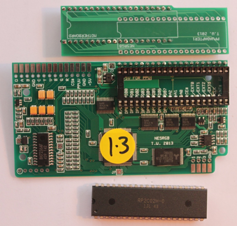
The following parts are included with the kit for the Famicom
AV.
|
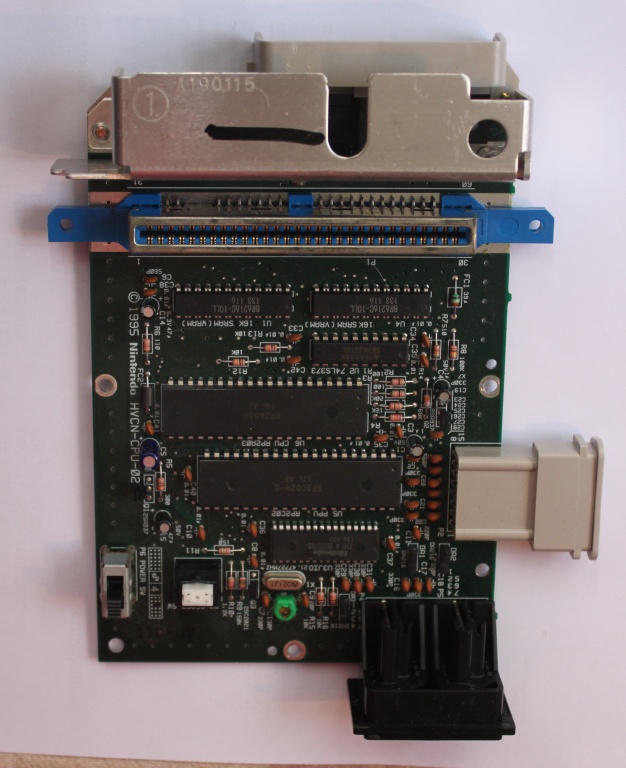 |
Open the Famicom AV with the special screwdriver and remove the motherboard. |
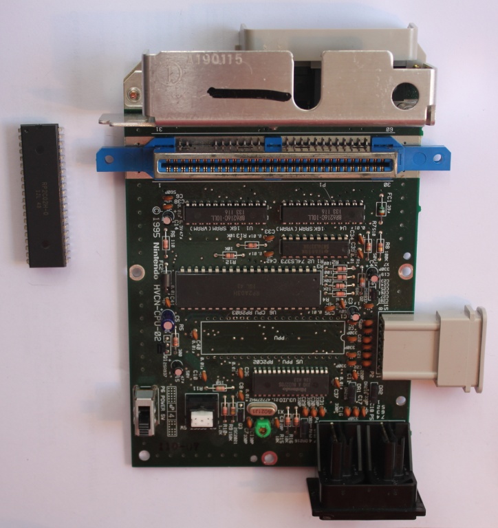 |
Desolder the PPU. This can be tricky because the motherboard's holes are plated through. Please read the article here: Desoldering the PPU. |
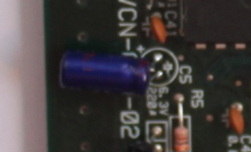 |
On this motherboard revision there is a capacitor, C5, located behind the PPU. This sticks up and prevents mounting the PPU adapter. Remove this capacitor (if it exists on your board), bend its legs over and solder it back in lying on its side. |
 |
Insert one of the 40 pin IC sockets into the motherboard in the
PPU's place. Then insert the round pin strips into the socket
strip and place the adapter board on top. Apply pressure so the
pins go into the sockets. Ensure a the pins are in the rows marked 'MOTHERBOARD'. If you install the adapter board the wrong way around or upside down it will not work! |
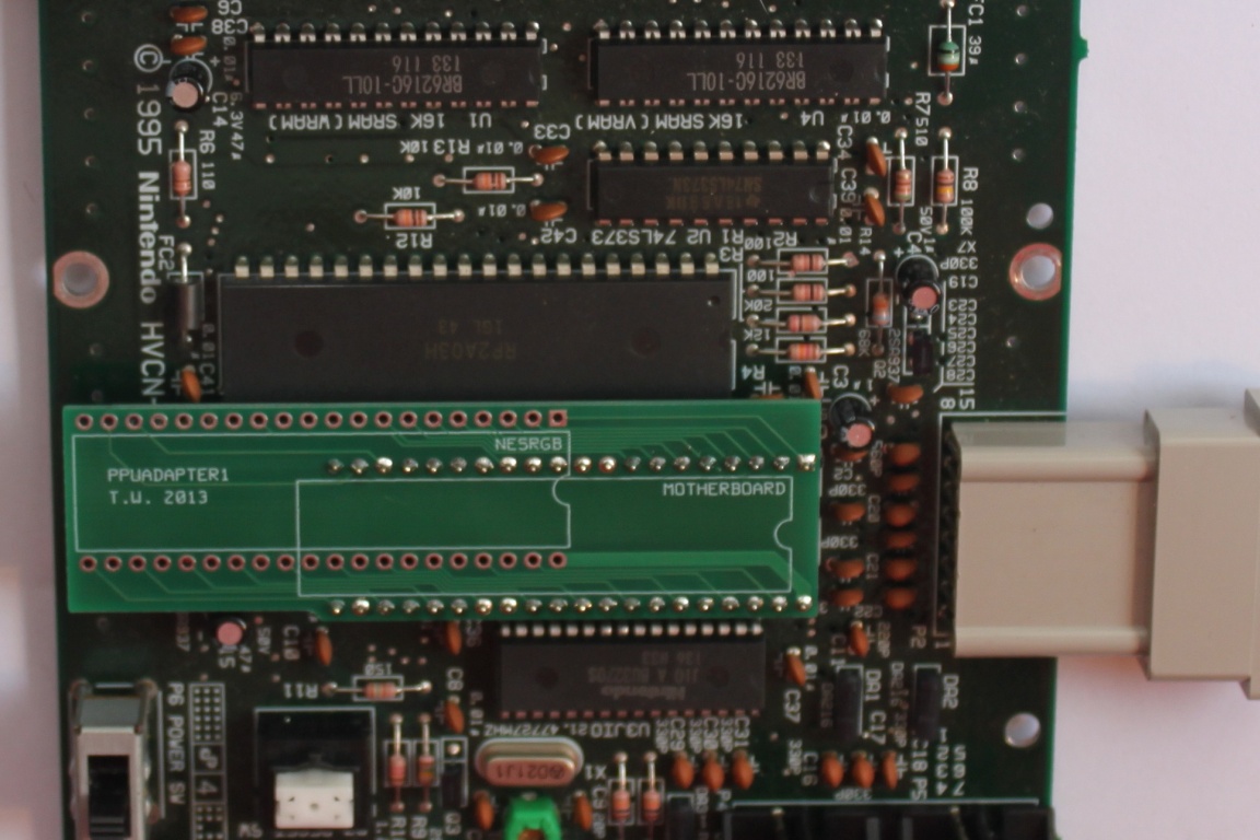 |
With a finger on the adapter board, solder the adapter board pins in place. Then turn the motherboard upside down and solder the 40 pin IC socket on the bottom. This way the pins will be straight and aligned correctly. |
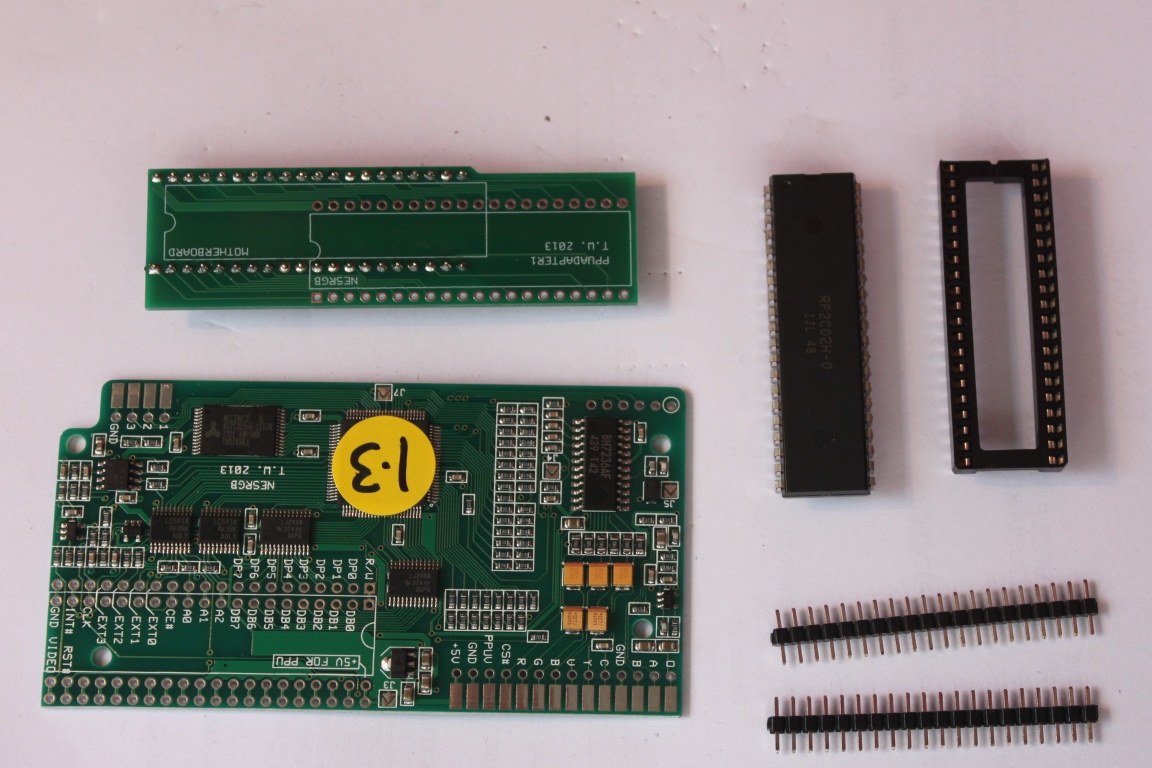 |
Gather the other parts of the kit:
|
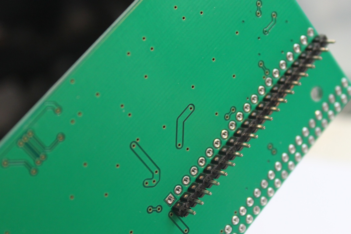 |
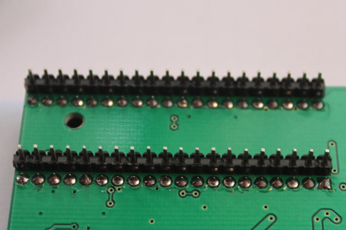
Insert the square pin strip into underside of the NESRGB board as shown. |
 |
Insert other other pin strip into the parallel position. |
 |
Solder the pin strip in place. |
 |
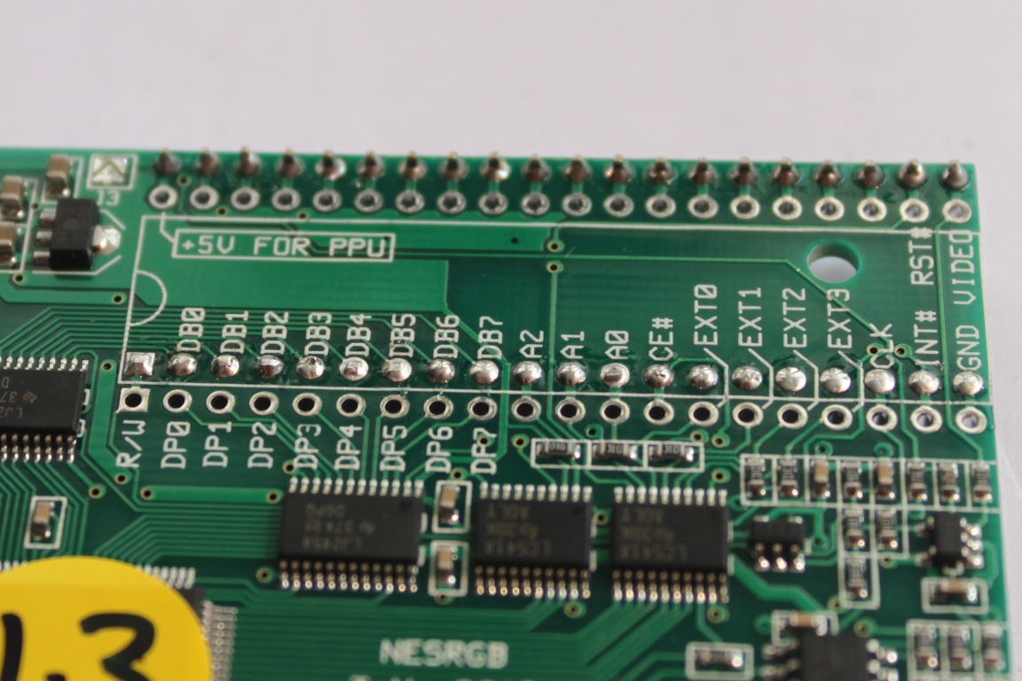
Insert the other 40 pin IC socket into the NESRGB board. Be careful to insert it the right way around. The adapter board and PPU are also pictured. |
 |
Solder the socket in place. Inspect the solder joints to make sure they are good. They will be difficult to access later. |
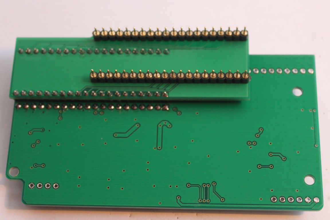 |
Solder the NESRGB board and adapter board together as shown. |
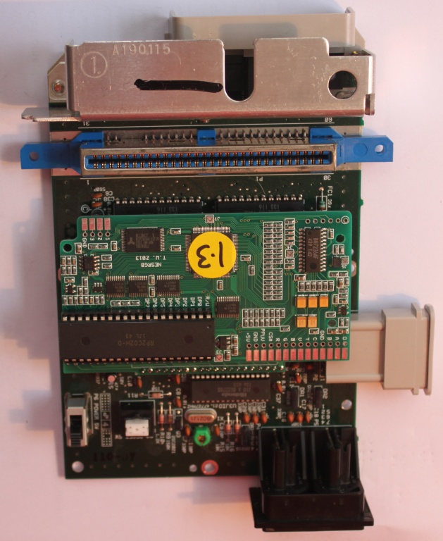 |
Insert the NESRGB board assembly into socket strip on the motherboard. Solder jumpers J3 (for power) and J5 (NTSC video). |
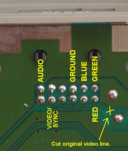 |
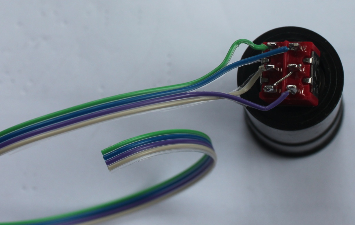
Now it's time to wire up the video signal. There are many
different ways to connect the video signal. I believe that most
people will want to use the Nintendo AV out port located at the
back of the console so that is the method I will describe here.
Red, Green, and Blue video signal are wired to the currently unused pins and the new encoded composite video signal is connected in place of the old one. You may also leave the original video line in place if you prefer. |
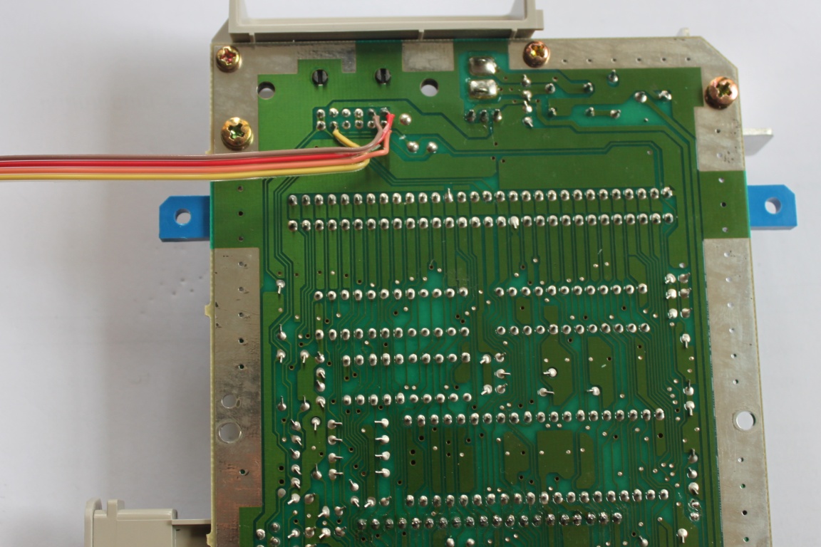 |
Wires are soldered to the connector pins. |
 |
The other end of the wires are soldered to the pads on the
NESRGB board. Solder jumper J3 to provide power to the NESRGB board. If you have an NTSC version NES you should solder jumper J5. If you have a PAL version NES, you need to solder jumpers J4 and J7. |
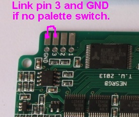 |
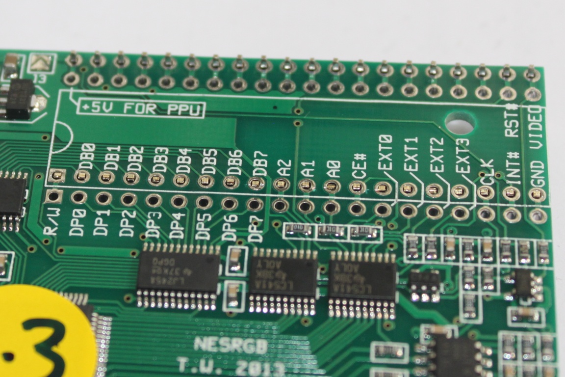
The NESRGB board features three palettes to choose from. This feature is optional. If you so not want a palette switch then bridge pin 3 and GND to permanently select the natural palette. |
 |
Wire up the palette switch. There are multiple ways to wire this switch depending on desired result. See the palette switch detail page. |
 |
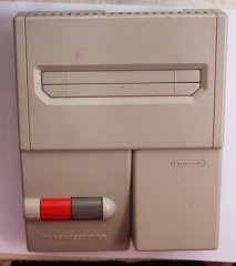
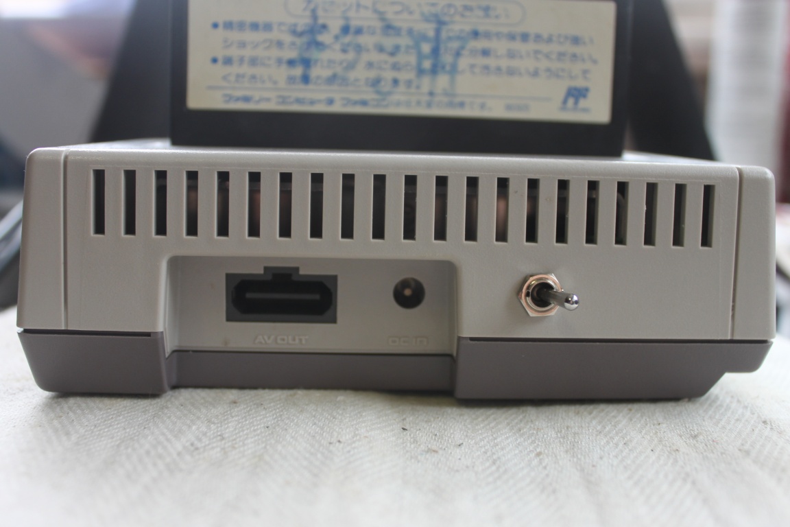
Drill a hole in the rear and mount the palette switch. Be
careful to choose a position for the switch that does not let it
collide with the heat sink when closing the case.
Older version of the kit were supplied with a four position slide switch. Some creativity is required to mount this one. |
 |
Reassemble the unit and test. A Gamecube SCART cable must be
used. The official Super Nintendo SCART cable will not work unless
it is modified before use (all 75 ohm resistors must be removed).
Japanese RGB 21 cables mat also be used but may require repair as they suffer from leaky capacitor problems. |
Change Log
30/8/2022 - Added link at the for NESRGB4.
15/2/2014 - Page created.
26/9/2014 - Updated.