RGB / S-Video upgrade for Nintendo NES
I developed a board that can be installed inside a NES or Famicom to improve the video quality. This is not a replacement PPU (Picture Processing Unit, the NES graphics chip) nor does require any parts from Nintendo arcade hardware. The original idea came from HardWareMan and thefox on the NesDev forum.
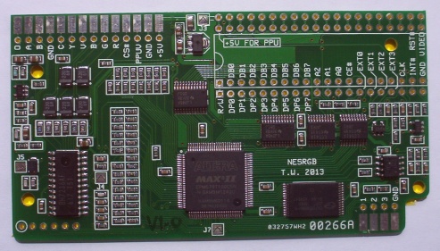
The NESRGB board effectively bypasses parts of the PPU - Palette RAM
(Color Generator), Decoder, and DAC. These functions are duplicated in
the NESRGB board with a focus on video quality. The timing of the video
is unchanged so there is no lag (no framebuffer, no VGA, no HDMI, etc,
etc), just non-interlaced 15kHz video output.
I have uploaded some high res screen shot photos here:
http://etim.net.au/nesrgb/announcement/photos/
Drakon has created video captures from the board (Youtube links).
Gimmick,
Castlevania 3, Kirby's Adventure
Full Castlevania 3
Playthrough
How it works (technical)
Refer to the operation block
diagram. The PPU part of the diagram is taken from US patent
number 4824106.
An Altera PLD sits between the PPU and the CPU data bus. When the CPU
writes data into the Palette Ram (Color Generator) the data is captured
and stored in the NESRGB board. Modified data is passed to the PPU. The
PLD also intercepts writes to the register controlling the operation of
the Multiplexer, making EXT0-3 outputs. The modified data passed to the
PPU removes data already available at the EXT0-3 outputs. The rest of
the information required (EXT4, blanking, and sync) is extracted from
the video output with comparators. The video data is then decoded from
the palette currently selected and passed out to the DAC and video
encoder.
Features
- User selectable palette. Three palettes available, I call them Natural, Improved, and Garish. The Natural palette has the same colours as the normal composite video output. It comes from the Nestopia NES emulator. Improved is from the FCEUX emulator. There is more variety in the colours. Some games look significantly better with this one. Garish is also from the Nintendulator but it is a palette from the Nintendo Playchoice PPU. It's very colourful indeed. More of a curiosity than anything else. There is a fourth choice - if no palette is selected the NESRGB board will 'turn off' and just pass data through. This way the NES will output composite video as if the board was not installed at all.
- Built in audio and video amplifier. Useful for the Famicom which does not have A/V outputs already.
- Outputs RGB, S-video (encoded from RGB), composite video (encoded from RGB), and composite video (original from PPU).
- Compatible with PAL and NTSC consoles (jumper selectable).
- Supplied with audio/video connectors, three position switch, and other assorted bits that may be required for installation.
- Size in mm 98.2 * 52.5 * 3.7
Installation
The NESRGB board is designed with the NES front loader in mind. It sits
in a socket where the PPU normally lives. The PPU is mounted in the
NESRGB board. See the picture below as an example (ignore the jumble of
wires soldered to the card edge finger at the bottom of the NES
motherboard, it is not related to the installation). It also shows a
separate voltage regulator board which is recommended for the original
NES because the its own voltage regulator heat sink is small and may get
too hot with the additional load from the NESRGB board.
The board may also be installed into AV Famicom and top loading NES models when a suitable pin adapter board is fitted.
Guide for
- Front loading NES
- Original Famicom - Updated for version 1.1 P/A board.
- Famicom AV - This info guide largely applies to the top loading NES.
- Famicom Twin
Switch wiring info - A three position toggle switch is now included instead of a slide switch.
Notes for version 4 - Updated installation guides are coming soon (end of August). Until then, refer to this for V4 installation info.
Where to buy
Buy from etim online shop
(Australia, International),
Updated
installer/distributor page.
For questions and comments please email.
![]()
Change Log
24/8/2022 - Added very basic docs for V4.
10/2/2019 - Added the link to the Software and Errata page.
27/9/2015 - Updated pinout and jumper diagram for V1.4 hardware.
9/12/2014 - New install guide for the original Famicom.
30/8/2014 - Added a install guide for the Famicom Twin
15/2/2014 - Added a install guide for the Famicom AV
30/12/2013 - Removed Paypal buttons, added link to new shop.
13/11/2013 - Added installation guide for the original Famicom.
22/10/2013 - NESRGB boards are temporarily sold out.
20/10/2013 - created.