Guide for installing the 2600RGB into a Atari 2600 Junior.
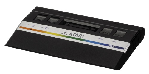
Tools and materials required:
- Soldering iron and leaded solder wire.
- Insulated copper 'hook up' wire. It's better to use wire that is thin and easy to work with.
- Solder sucker or desoldering iron.
- Pliers and cutters and screwdrivers and tin snips.
- Drill with a 12mm step drill bit.
- Two part epoxy glue (Araldite or similar).
- Electrical tape.
- Hot glue gun.
Click on the pictures to make them bigger.
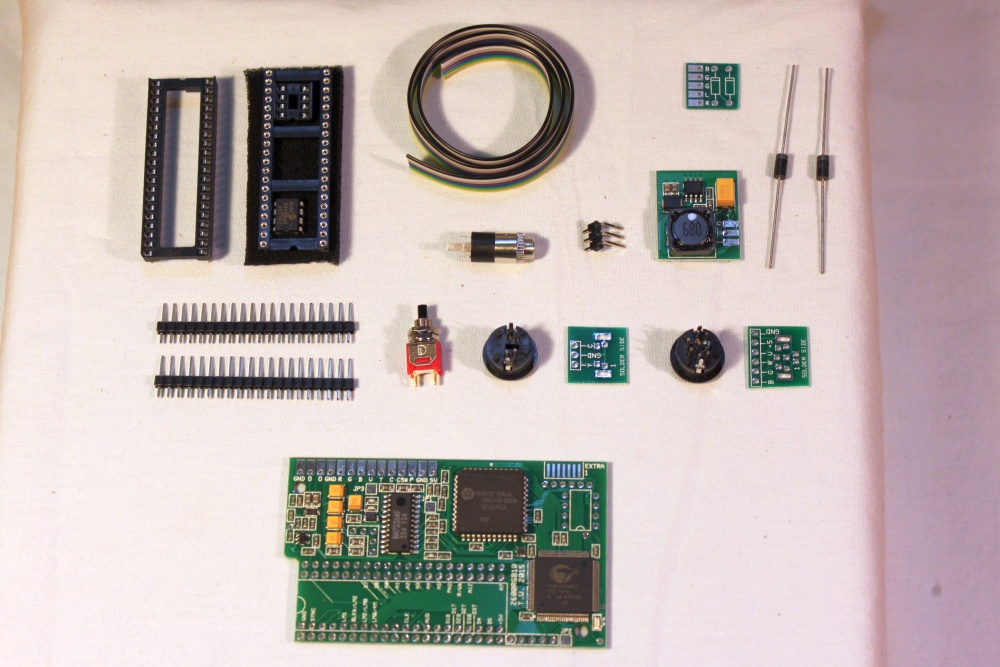 |
Look at all the parts you get!
|
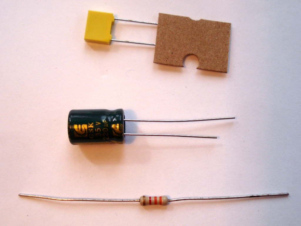 |
In addition to the above,
|
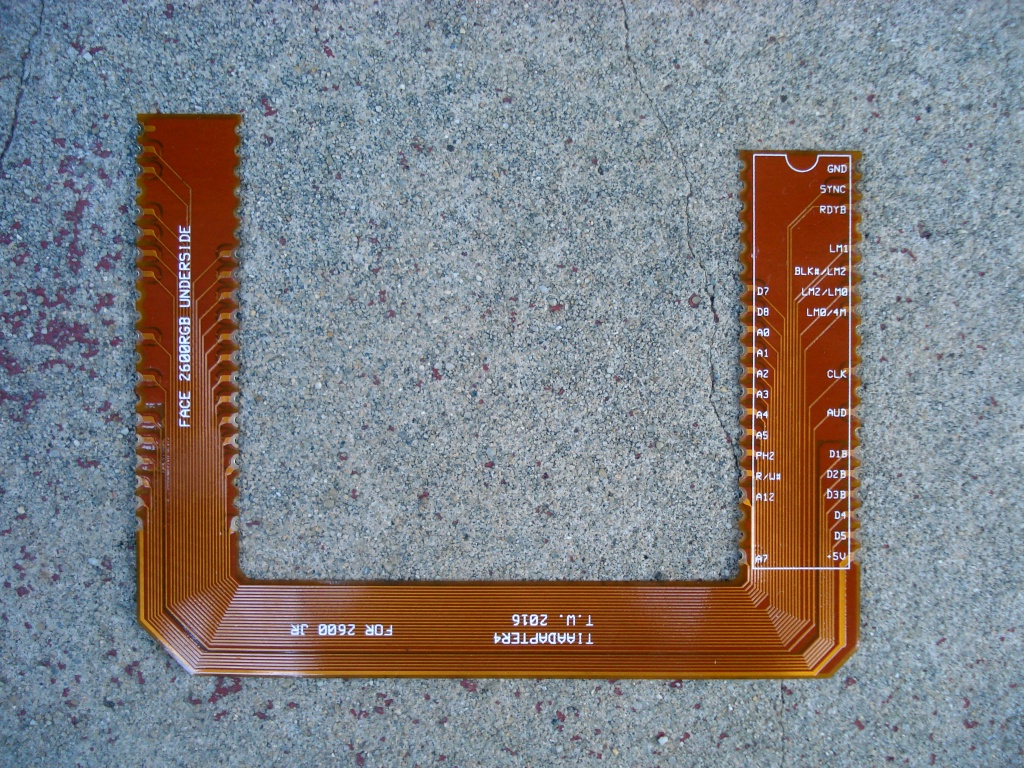 |
And finally, the flex adapter. |
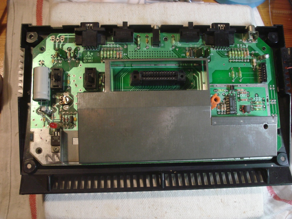 |
Take some screws out of from the bottom. Most of the motherboard
is covered by a metal RF shield. Normally there is another,
separate metal piece over the RF modulator section to the right,
but I seem to have lost that one. |
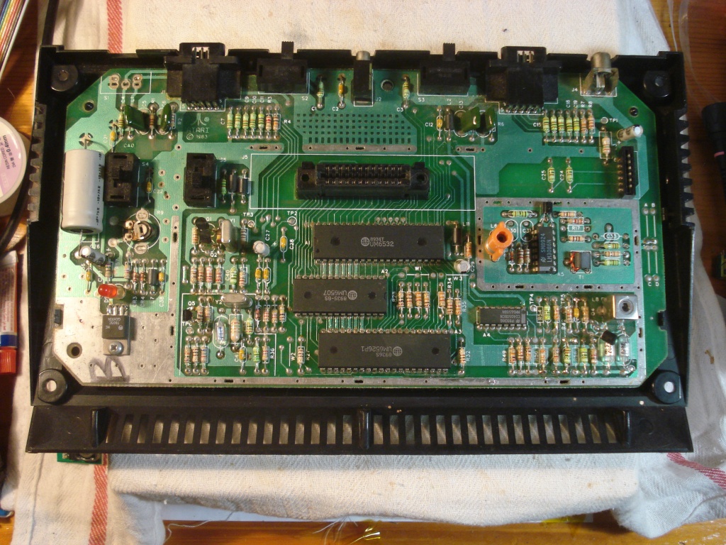 |
The two halves of the metal straightening the little tabs on the
underside. The TIA (Atari graphics chip) is the 40 pin DIP package closest to the edge of the motherboard. The NTSC version is labelled C010444 or UM6532. The PAL version is labelled C011903 or UM6526. |
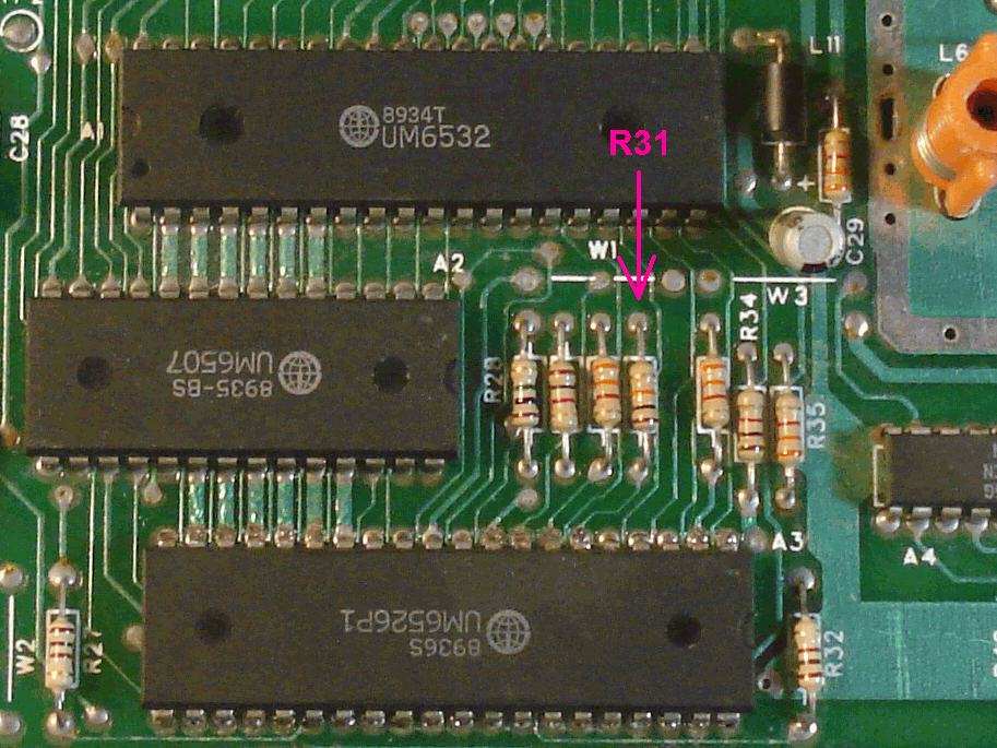 |
If your console is the PAL
version you must locate R31 which is a 10k
(brown-black-orange) resistor. In the PAL version of every other
Atari 2600 model this is a 3.3k (orange-orange-red) resistor. The
wrong value appears to been fitted by mistake here. For correct
operation of the 2600RGB board, this resistor must be replaced
with the 3.3k value one supplied in the kit. The NTSC version console is not affected as the NTSC version of the graphics chip does not use the output connected to this resistor. |
 |
This is where the 2600RGB board should be mounted. Above the
motherboard, between the two grey capacitors C27 and C29.
Capacitor C29 may need to be bent to the right slightly to allow
the 2600RGB board to fit. Before the 2600RGB board is mounted it must be prepared. |
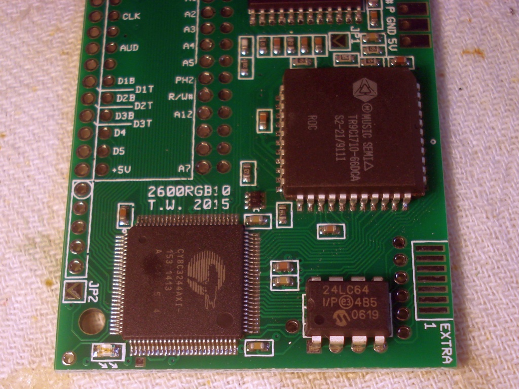 |
Solder the serial EEPROM in place on the 2600RGB board. The IC
socket is not used for reduced height. |
 |
Cut the pointy legs off the EEPROM that poke through the 2600RGB
board. This prevents the sharp legs from scratching the flex
adapter. |
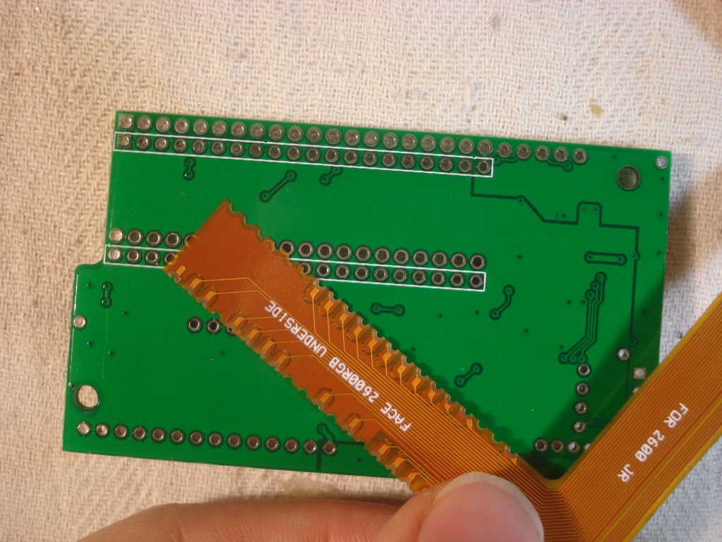 |
Find the flex adapter. One side is slightly narrower and is
marked "FACE 2600RGB UNDERSIDE". |
 |
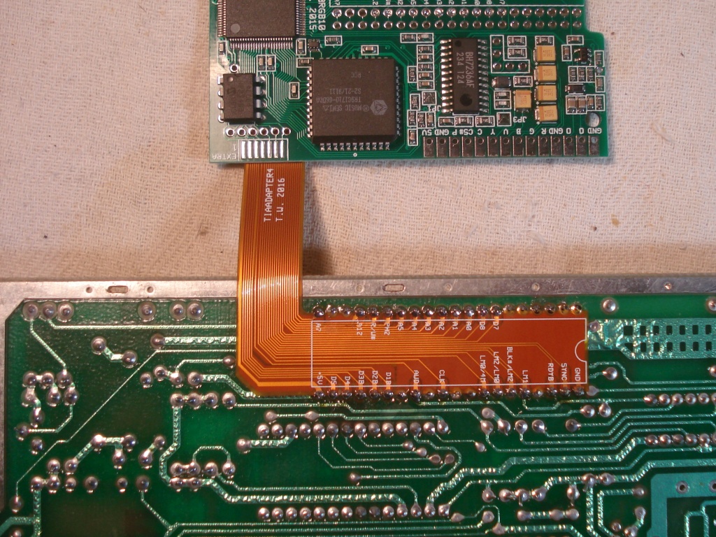
Solder the flex adapter in place to the underside of the 2600RGB
board as shown. Only the pads with labels need to be soldered. |
 |
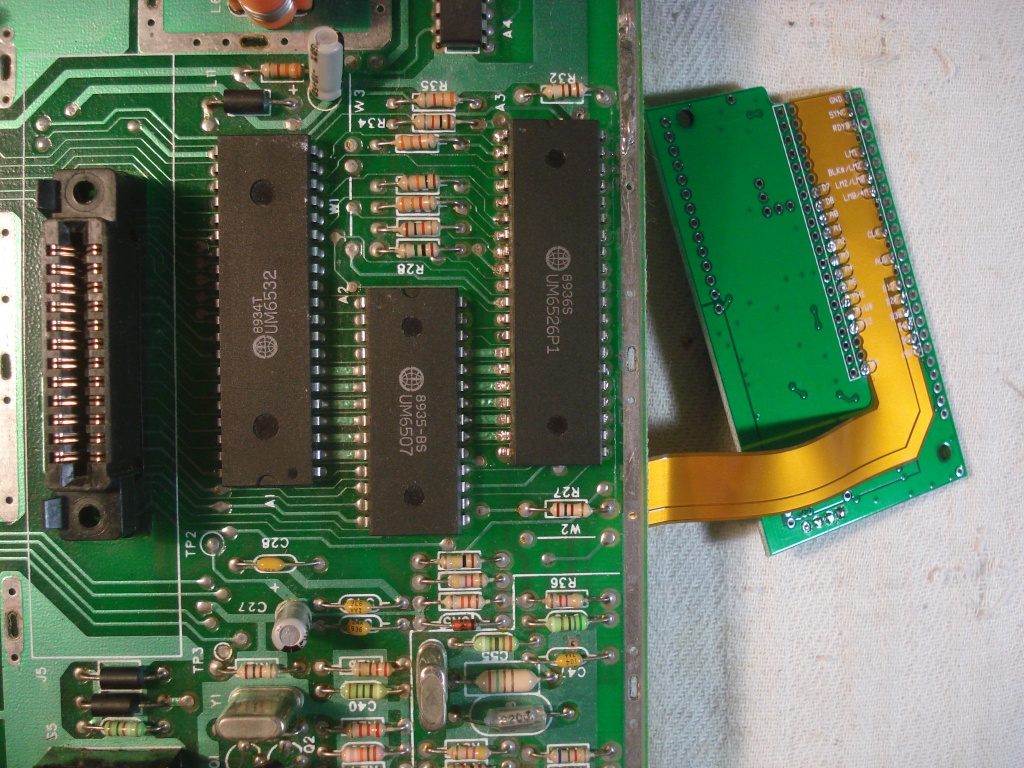
The other end of the flex adapter fits between the pins of the TIA on the underside of the motherboard. Make sure it is aligned correctly and solder it in place. Only the pads with labels need to be soldered. |
 |
Carefully turn over the tethered pair of boards then go and
fetch your sharpest pair of side cutters. |
 |
There are four signals that must be routed through the 2600RGB
board for it to function correctly. The signals are RDY, D1, D2,
D3. TIA pins 3, 15, 16, 17 need to be cut in such a way as to disconnect them from the motherboard. A wires is soldered to each of these pins, the other end of which is soldered its associated pad on the 2600RGB board, RDYT, D1T, D2T, D3T, respectively. |
 |
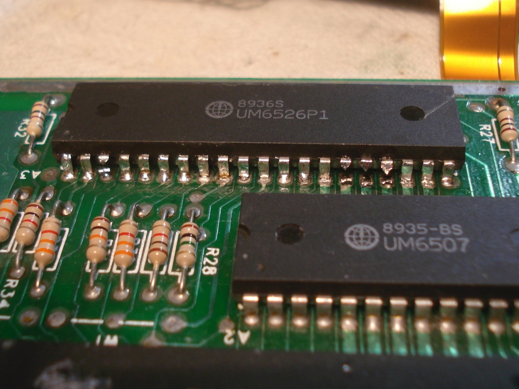
Position the cutters around the pin. The cut should be made
slightly below the bend in the pin. Once the pin is severed press
down on the cutters and bend the cut off part of the pin down to
the motherboard. Avoid placing any stress on the remnant of the pin on the chip. |
 |
TIA pins 3, 15, 16, 17 have been cut. |
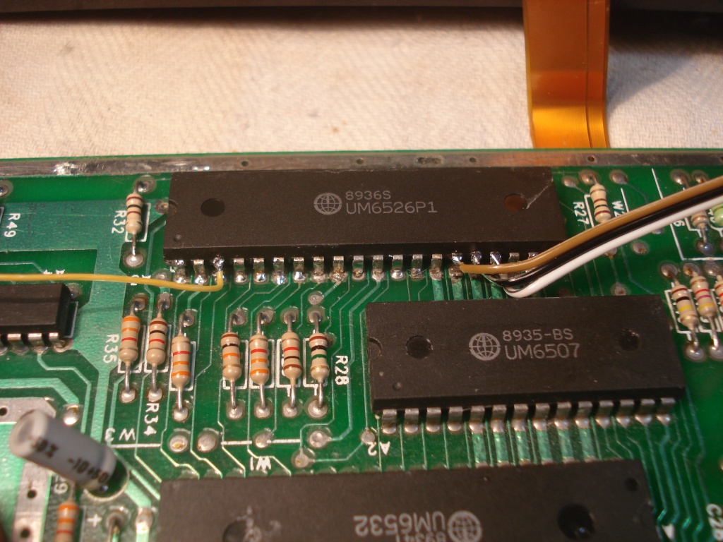 |
Solder a wire to each of the four pins. It's helpful to use
wires of different colours of you have them. |
 |
Place the 2600RGB board over the motherboard as shown. Solder
the wires from TIA pins 3, 15, 16, 17 to the equivalent points on
the 2600RGB board RDYT, D1T, D2T, D3T respectively. Note that the
RDYT pad is not labelled on the 2600RGB board. Use four points of hot glue to hold the 2600RGB board in this position. Hot glue is ideal for this task as the bond will hold the board in place reliably but may be broken by applying force if changes need to me made in future. |
 |
Strip the insulation from the seven wire ribbon cable. Tin the wires with solder and do the same to the pads labelled EXTRA on the 2600RGB board. Solder the wires by holding the ribbon in place and applying pressure with the soldering iron tip, one at a time. |
 |
Cut the ribbon cable to length and wire it to the left
controller port according to the wiring diagram. The pin listing for the Extra connection is,
|
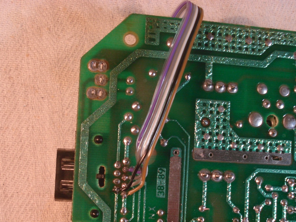 |
Wires from the Extra connection pins 3-7 connect to the left joystick port. |
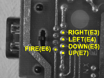 |
For reference. |
 |
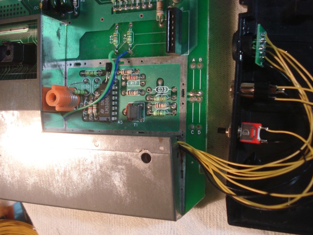
The RGB video output connection needs to be mounted somewhere.
The most reasonable space seems to be at the side of the console. Use a step drill bit to drill the 12mm hole for the 8 pin mini din connector. Before drilling, screw both halves of the shell together. It's no problem if part of the hole is cut into the bottom half of the shell. As long as it's mostly in the top half it will be fine. Use two part epoxy glue to hold the mini din connector in place. |
 |
Mount the audio jack socket and palette switch if required. |
 |
Wire up the audio/video output connectors according to the 2600RGB
wiring diagram. Now is a good time to test the console. Remember that you need the top shell fitted to be able to insert most cartridges into the cartridge slot. |
 |
Put the metal shield back on now. You will need to cut some
holes in to it for the wires to escape. |
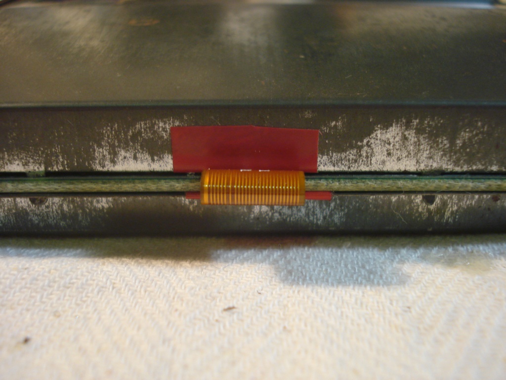 |
Also, place some electrical tape around the parts of the metal
shield which will contact the flex adapter. This may not be
strictly necessary, but it's a good idea in case the shield has a
sharp edge. |
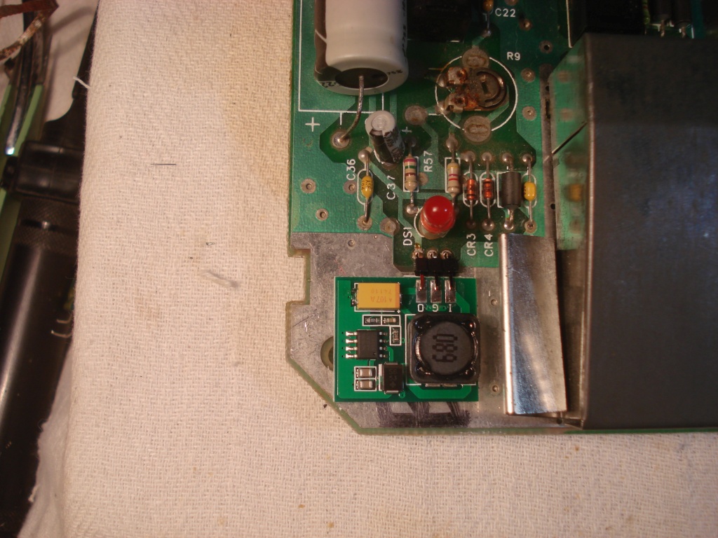 |
The last thing to do is replace the linear voltage regulator
with a more efficient switch mode type. This is required because
the console requires more power to operate with the 2600RGB board
installed. If the linear regulator was left it place it may
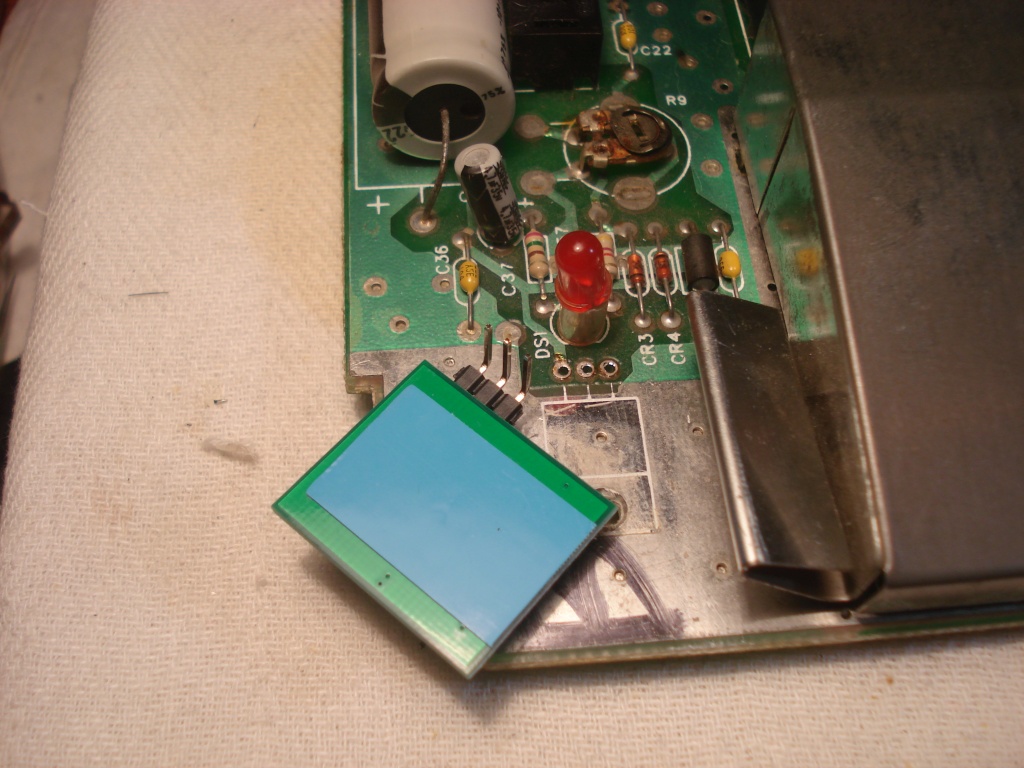
overheat after a while. Find the linear 7805 three terminal regulator and remove it from the motherboard. Clean the solder out of the holes with a solder sucker. Bend the metal shield away from the area to allow the switching regulator to fit. Then insert the 3p right angle pin header into the regulator holes as shown, bent part into the motherboard. Align the short end of the header with the pads on the switching regulator and solder them into position (don't solder to the motherboard yet). |
 |
Make sure the area is clean and dirt free. Remove the plastic which covers the sticky adhesive on the back of the switching regulator. Stick it to the motherboard and solder the pins. |
 |
The pins of the switching regulator are labelled I for input, G
for ground, O for output. After you have stuck and soldered it in
place, I recommend testing the ground connection with a
multimeter. Measure the resistance between a ground point (such as
the large copper plane beneath the regulator) and the G pad to
check it is close to 0 ohms. If it is not connected please solder again. The Atari may be damaged if it is powered on and the regulator is not connected properly. |
 |
An extra capacitor is required to reduce radiated noise. Install
the supplied 220u electrolytic capacitor between the Input
and Ground pins of the
switching regulator. The negative leg (marked with a stripe) is
connected to ground. That's it. Put the console back together. |
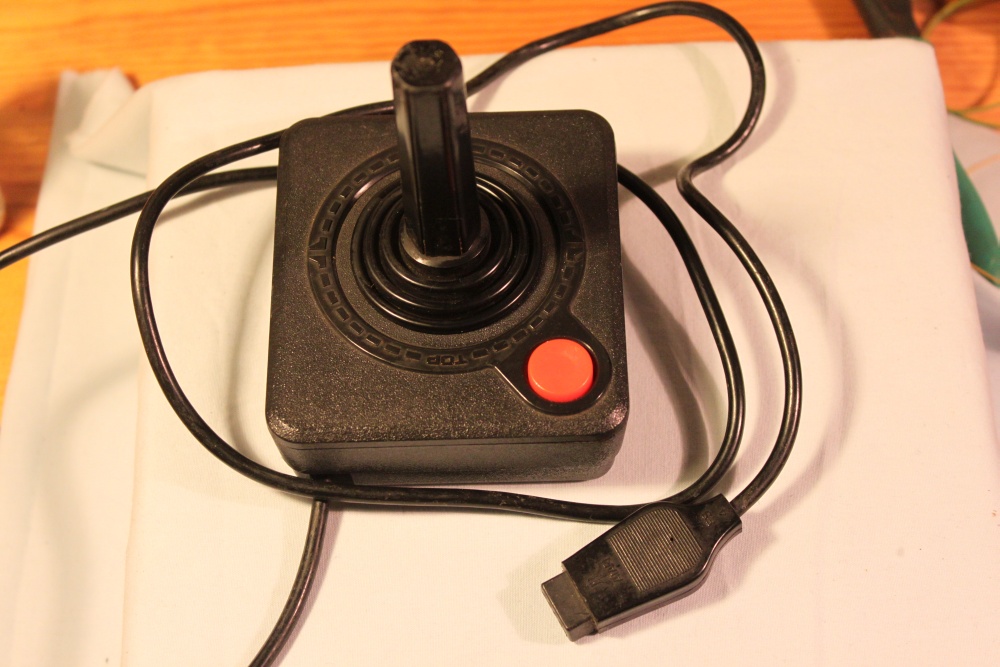 |
Now to install the extra button on the controller. When pressed,
it will assert the left and right joystick signals simultaneously.
The Extra button is pressed while performing another action. This
normally impossible combination of signals is detected by the
2600RGB board. Extra + Up = Select. Extra + Down = Reset. Extra + Fire = Palette switch. |
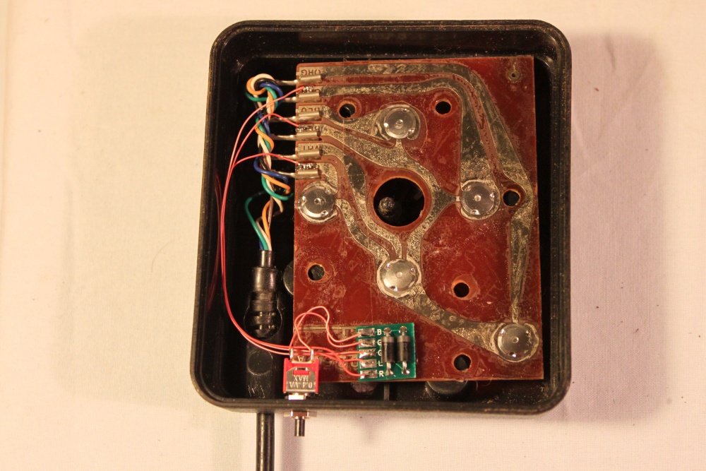 |
Drill a 5mm hole (twist drill bit is fine) to in the joystick
and mount the pushbutton in a convenient spot. Solder the two
diodes to the diode board and install according to the wiring
diagram. You can mount the diode board with double sided tape or
similar. There are five pads on the diode board. Button, Ground, Ground, Left, Right. Solder the pushbutton between the button an ground terminals. Then solder the ground, left, and right terminals to the joystick board. You can identify the ground connection easily because it's the only one that connects to all the switches. The left and right points should be obvious from looking at the board layout. |
Change Log
30/11/2016 - Page Created.